

Enterprise
Siemens and NVIDIA Bring PCB Inspection Into the Digital Twin
Siemens and NVIDIA's virtual PCB inspection workflow uses digital twins and synthetic images to prepare quality checks before physical production.
Mainstay Communications Team · · 1 min read
In brief
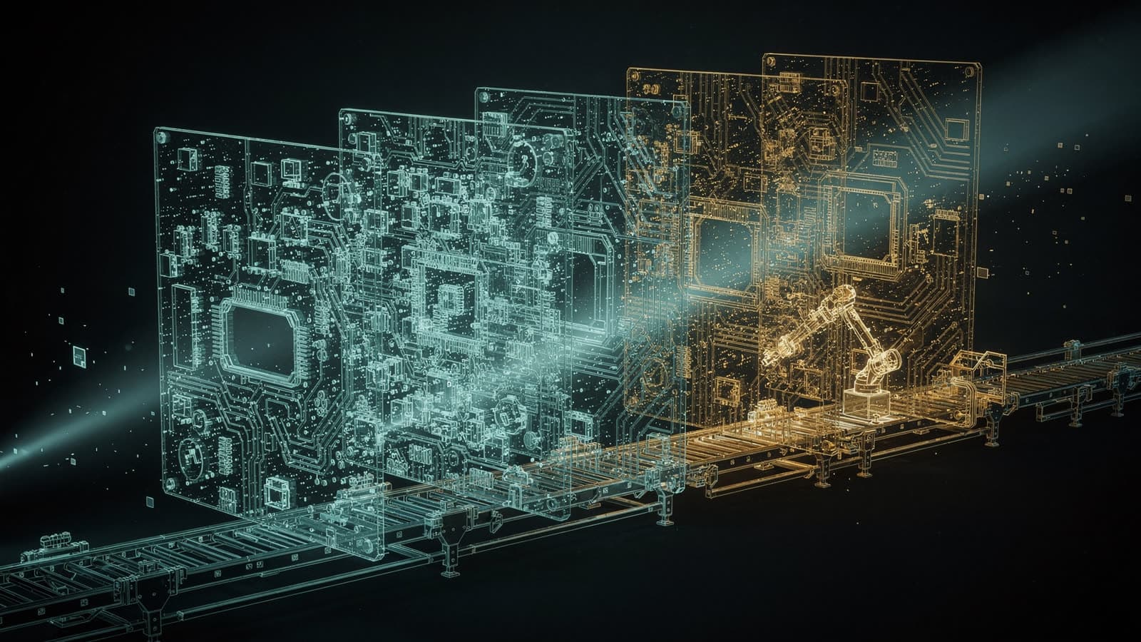
Siemens and NVIDIA are developing a workflow that prepares automated optical inspection from a digital representation of a circuit board. The collaboration is being demonstrated at Siemens' electronics factory in Erlangen, Germany.
How does virtual PCB inspection work?
Virtual printed circuit board (PCB) inspection uses a digital reference board and synthetic images to prepare optical quality checks before physical boards arrive. Siemens' announcement connects Teamcenter, Process Preparation X and NVIDIA Cosmos to build that workflow from design and component information.
The workflow also includes AI-supported secondary inspection to help distinguish real defects from false alarms during production.
Siemens lists targets including up to 85% less manual engineering effort for inspection programming and more than 5% improvement in first-pass yield. These are project targets, not established results across customer factories.
The question for manufacturers
Our read: a useful demonstration should follow one board revision from engineering data through inspection preparation. Buyers should ask which inputs need cleanup, how defects are selected and how performance is checked against physical samples.
That gives a technical sales team a concrete story to show: the input, the virtual preparation and the production decision. Keep the target metrics attached to their test conditions so a compelling visual doesn't become an unsupported performance promise.
Sources
Companies mentioned
Mainstay Digital · Spatial and 3D visualization for industrial companies